Laser Assisted Bonding
The soldering of electronic components in very individual solutions. The use of lasers is a real alternative to reflow soldering, especially for complex electronic components such as flip chips.
The soldering of electronic components in very individual solutions. The use of lasers is a real alternative to reflow soldering, especially for complex electronic components such as flip chips.
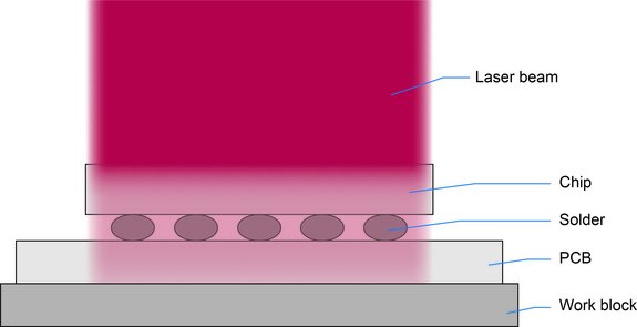
Flip chip assembly, also known as controlled collapse chip connection (C4), is a process for contacting unpackaged semiconductor chips using bumps, i.e. contacting hills. The chip is mounted without further connecting wires, with the active contacting side facing downwards, hence the name flip chip or BGA (ball grid array). For very complex circuits, flip-chip mounting is often the only sensible connection option because several thousand contacts often have to be realized. This means that the entire surface can be used for contacting. In order to bond the chips, laser assisted bonding - LAB for short - is increasingly being used alongside other established processes with specially adapted Laserline diode laser system solutions. Direct chip attachment applications with dimensions of 3 x 3 to 100 x 100 mm² and material thicknesses between 50 and 780 micrometers are used in modern mass production.

Laser assisted bonding (LAB) from Laserline offers advantages over conventional bonding processes such as mass reflow ovens. The precise application of energy with our OTZ zoom optics results in lower thermal stress and therefore significantly reduced warpage. This approach is particularly suitable for thin substrates and offers excellent stability with different package types. LAB solutions also contribute to a significant reduction in manufacturing costs as they consume less space and energy compared to reflow oven solutions. At the same time, our laser-assisted bonding solutions ensure high throughput.
These Laserline systems are often used together in LAB applications
Would you like to find out more about Laser-Assisted-Bonding?
Send us your request!